


News
EconoMISER Scales Up Geopolymer Capabilities
A range of key workstreams have been identified by the Foundation Industries Sustainability Consortium, as particularly high-impact areas of research for FISC partners
Lucideon Expands with New Offices in Japan
Lucideon is targeting international growth with expansion in the Japanese market, with additional offices in Osaka and Haneda Innovation Park
Leaders Explore Low Carbon Innovation in UK’s Foundation Industries
Exploring opportunities to drive low carbon innovation in the production of vital materials used across everyday life
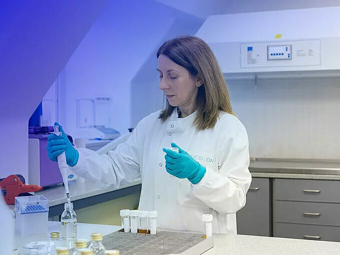
At Lucideon we provide material solutions to the toughest problems
We use our capabilities, expertise, and technologies in materials science, testing, and assurance to overcome the most complex challenges and deliver innovative solutions.
We are a trusted partner, providing unrivalled technical consultancy to enable, enhance, and accelerate our clients’ R&D activities.
We are passionate about making the world a materially better place and we strive to lever the trailblazing talent of our people worldwide to optimise environmentally-focused application of resources and energy.
Consultancy
When you encounter a really challenging materials or product development challenge, it’s good to know there is someone out there who can help. We will work with you to understand your issue – and then solve it. We offer a range of types of consultancy from Failure Analysis, Materials Selection / Characterisation / Development, to Process and Product Optimisation. Typical areas of application include Additive Manufacturing, Net Zero, Traditional Ceramics, Advanced Ceramics, Microbiology, Fuel Cells, Batteries, Nuclear Power, or Refractories.
We also offer access to our consultancy expertise via our Technology Partnerships – we are proud to have over 60 partners worldwide.


Our Expertise

We pride ourselves on the materials experts and scientists that work at Lucideon - as well as being highly qualified, they also have the hands-on practical experience that makes them world-renowned professionals in their own field.

Lucideon's training courses have been developed by our in-house experts, all of whom have years of industry and practical experience. We offer a selection of courses, covering a wide range of ceramics and refractories subjects.
Our Technologies
We lead the way in the development of novel materials technologies. We work collaboratively, partnering with you to adapt our novel technology platforms to your products and applications. And, if you're developing technologies of your own, our R&D team works with you to optimise and bring them to market quickly.
We have several proprietary technology platforms:

Our Capabilities
Complementary to our consultancy capabilities, we provide materials & products testing, characterisation, analysis & evaluation to customers around the world across a wide range of industries.
Lucideon is home to The AMRICC Centre, a hub for companies to seek technical support on their product development and commercialisation journey.
Our IMPACTTM capability provides computational tools to enhance the materials research & development lifecycle.
We also offer assurance services through Lucideon CICS Limited, a leading global provider of sustainability assurance and management systems certification.
We manufacture and supply ceramic Colour Standards – these are internationally recognised as the leading standards for use in colour measurement and calibration.
Testing & Characterisation
Unlike other test houses, we don't just provide data; our experts offer analysis and evaluation to provide answers to your questions, ensuring that you have the full picture.
The AMRICC Centre
Lucideon runs The AMRICC Centre on behalf of its partners providing leadership and hosting its facilities at its Stone site
Integrated Materials Processing and Computational Techniques (IMPACT™)
Clients come to Lucideon for solutions to some of the riskiest and time-consuming parts of the R&D lifecycle. IMPACTTM involves the identification of new materials, reformulation of existing products, and development and optimisation of new processes.
Assurance
Our verifiers and auditors in Lucideon CICS Limited are renowned for their expertise and well-planned and executed verifications to comply with voluntary and mandatory standards across a range of industries.
Colour Standards
Accurate colour measurement is vital to the production process in many industries. Produced using leading-edge ceramic technology, our colour standards are stable, durable, and easy to use.
Insights
Here you’ll find Lucideon’s stories, case studies, latest news, webinars and events calendar. Registered users can also view or download our white papers.

Discover more about some of the amazing work we are doing

Read our case studies about previous work

Latest news releases and news archive
Discover our Industries

Aerospace
Consultancy, materials development, and testing throughout the aerospace, space and defence supply chain
Ceramics
Materials and process development for the advanced ceramics and traditional ceramics sectors.

Construction
Laboratory and on-site consultancy and testing of construction products, systems and structures

Energy & Nuclear
Materials development and testing for the power generation, wind, nuclear, fuel cells, and oil & gas sectors

Healthcare
Materials development, technology & testing for the medical device, pharma & consumer product sectors

A career with Lucideon
Joining our team puts you in the company of scientists who have grown with us to be world experts in their fields. A career with Lucideon will mean you continuously hone and extend your skills and knowledge, not only in science but in business too. Our consultants build close, long-term relationships with clients and take responsibility for delivering revenues for the business.
We are proud to be a trusted delivery partner to some of the world’s iconic brands, all of whom are leaders in their respective markets